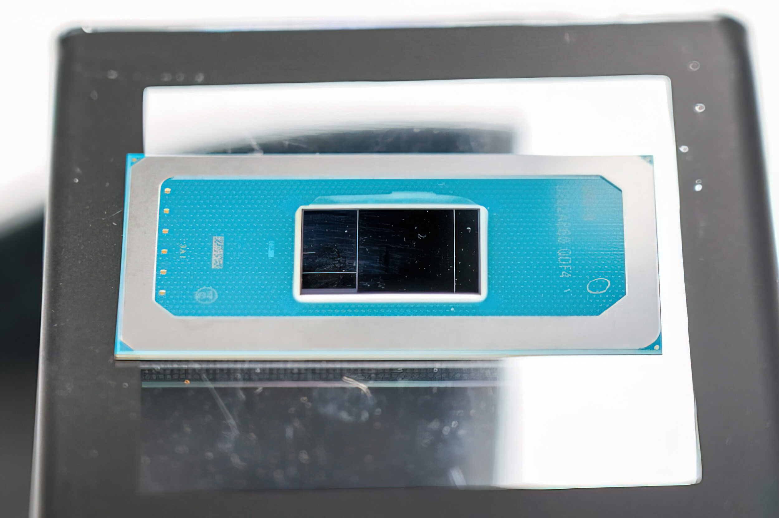
Intel InnovatiON 2023 event is currently ongoing and part of the key announcements for this year’s showcase is Meteor Lake: announced as part of Intel’s IDM 2.0 strategy, Intel will be moving from monolithic designs to disaggregated design moving forward and the first processors to use such a design is Meteor Lake.
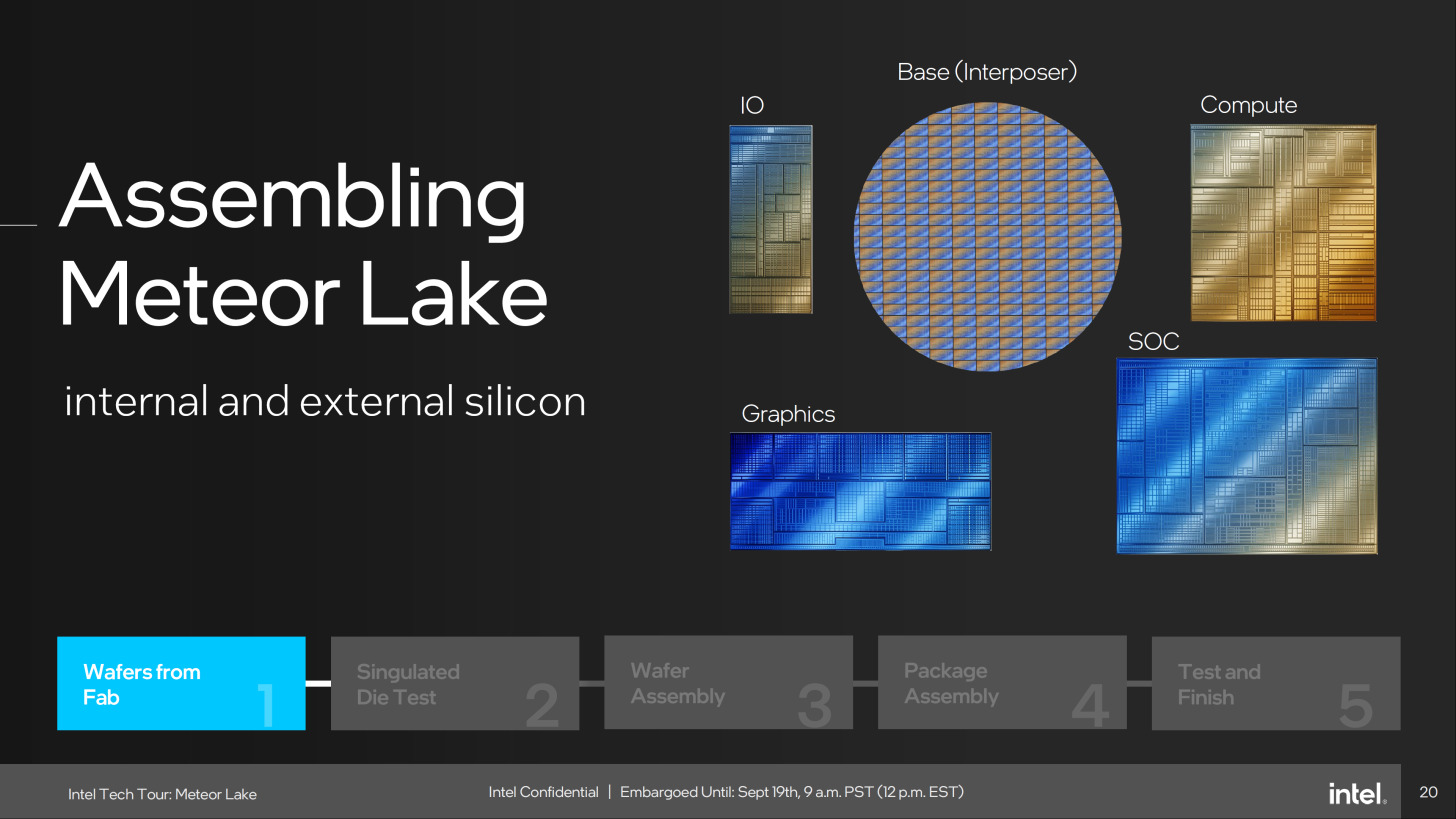
Disagreggated is Intel’s term for its tile-based approach or what we know right now as chiplets. Whether you call them chiplets or tiles, the common theme on both is that they separate die-level components and split them into multiple tiles or chiplets, and then identifying those components that would benefit from being built on a modern node (Intel 4) while fabricating other components on older nodes (TSMC N6). In the case of Meteor Lake, Intel’s own inhouse fab will be making their compute tiles for both P-cores and E-cores while the rest of the tiles (SoC, Graphics, I/O) could be built on older nodes or external or fabs.
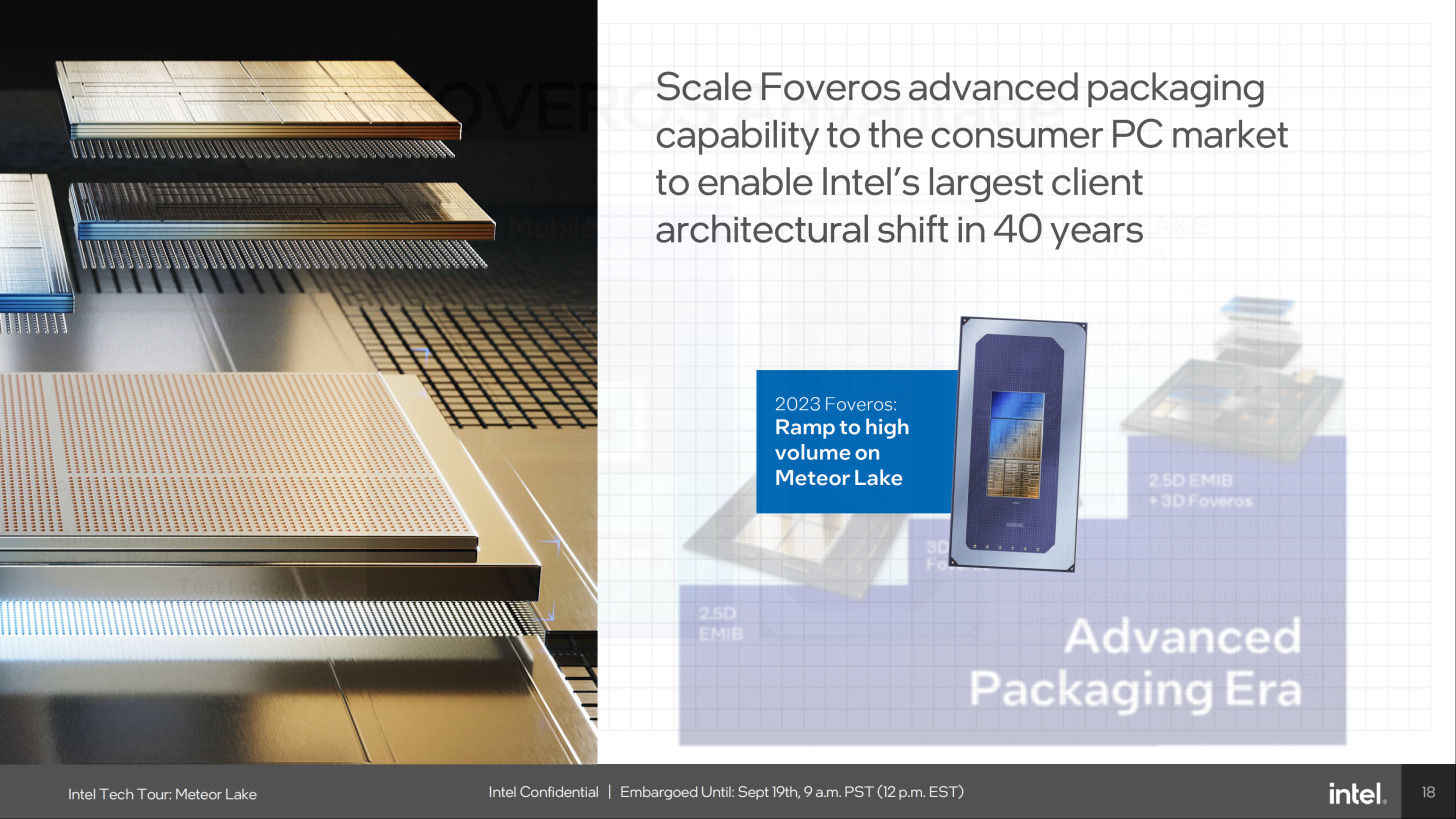
The main challenge here is providing similar if not better latencies between tiles versus if it was made on a single die. Intel will be utilizing their Foveros packaging technology to tie all the dies together to bring a modern CPU that offers the advantages of Intel’s tiled desIgn but also gives Intel the benefit of moving at a pace to allow them to improve their Intel Foundry Services as well by allowing them to advance their key components while relegating secondary components to another node or foundry.
Let’s take a closer look at the various components and technologies that Intel is introducing with Meteor Lake in this article.
Meteor Lake is slated for launch on December 14, 2023.
Why Go with Tiles?
While this is corporate PR to side-step potential eyebrows raising on why Intel chose to go with tiles which goes against the grain of their aggregation step when they started putting together components like the North Bridge onto the die itself, it make sense in a way. Intel differentiates their Meteor Lake tiles from what is referred to as a multi-chip module or MCM by way of putting processor components onto tiles and less with standalone components.
Let’s just take it as it is: it is more cost-effective for Intel to go with this approach for many reasons primarily because they’ll be saving themselves some effort in creating the parts themselves all the while mastering packaging that allows them to offer this kind of service down the line via their foundry business.
Regardless of intent, it does look good on paper and we already have AMD utilizing chiplets to set a benchmark on what can be done with such an approach.
Intel’s approach with Meteor Lake represents a departure from traditional monolithic designs. This shift is driven by the need to accommodate three distinct logic devices within the processor: the CPU, iGPU (integrated graphics processing unit), and NPU (neural processing unit). Each component requires substantial bandwidth and processing power, prompting this unique arrangement.
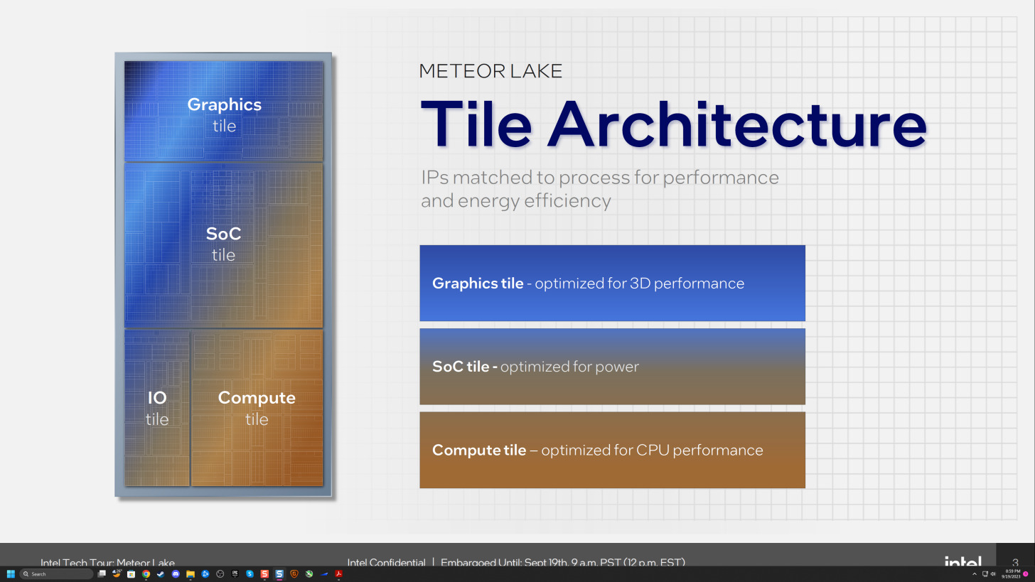
Meteor Lake comprises of four primary tiles or chiplets, alongside a base tile acting as an intelligent interposer. This interposer plays a pivotal role in facilitating high-density, low-latency connections between the chiplets. These primary tiles consist of the Compute tile for CPU cores, the SoC (System-on-Chip) tile housing the NPU, memory controllers, and other critical components, the Graphics tile for graphics rendering, and the I/O tile managing various physical interfaces.
This innovative disaggregated design departs from the conventional monolithic approach. While it may seem complex, it offers advantages such as improved efficiency and scalability. Meteor Lake’s launch could possibly mark a significant step forward in CPU architecture, aligning with industry trends seen in chiplet-based designs.
Tile Make-Up and Overview
As mentioned, Meteor Lake will comprise of four primary tiles with the key tiles being the Compute tile. Take note that Meteor Lake that while I say key, its parts are all vital in the processor’s operation.
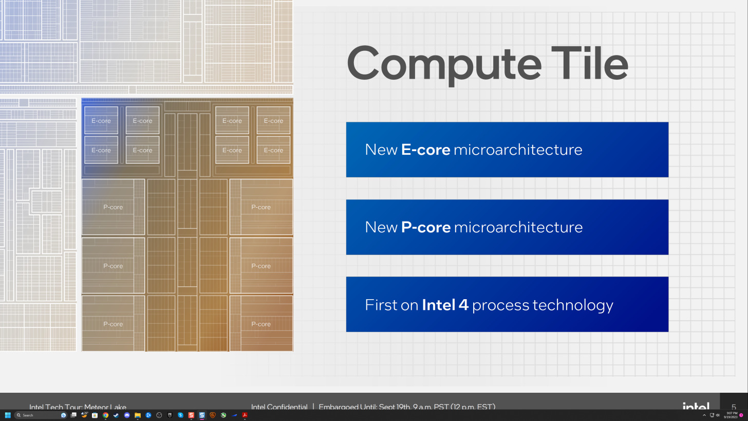
The Compute tile serves as the hub for crucial CPU cores in Meteor Lake. This tile is constructed using the latest Intel 4 foundry node and comprises four essential components: Performance Cores (P-cores), Efficiency Cores (E-cores), an L3 cache, and the ringbus interconnect.
Intel introduces the “Redwood Cove” performance core with Meteor Lake, aiming for significant improvements in IPC, clock speeds, and ISA capabilities compared to the current “Raptor Cove” P-cores. In a Meteor Lake Compute tile, there are up to six P-cores at most.
Alongside the six P-cores, the Compute tile houses two E-core clusters, each featuring four cores. Meteor Lake introduces the new “Crestmont” E-core, promising enhanced performance per Watt and IPC compared to the current “Gracemont” E-core. While “Redwood Cove” P-cores support SMT (HyperThreading), the E-cores maintain a 1:1 logical processor per core configuration.
Each “Redwood Cove” P-core boasts a dedicated L2 cache, while the two “Crestmont” E-core clusters share an L2 cache among their four cores. Both the E-core clusters and P-cores share a unified L3 cache exclusive to the Compute tile.
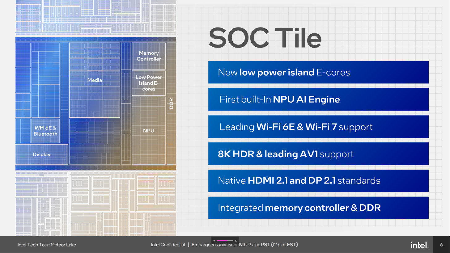
The SoC Tile, strategically positioned at the heart of the processor, combines several vital components that once belonged to the uncore section of the chip. Notable inclusions consist of the memory controller, the NPU responsible for AI Boost acceleration, the media accelerator, the image processing engine, the display controller, and the I/O interface.
This tile features two distinct fabric types, catering to various device interconnections. Intel introduces the network-on-chip (NOC), a low-latency, coherent fabric designed for linking high-bandwidth devices within the SoC tile.
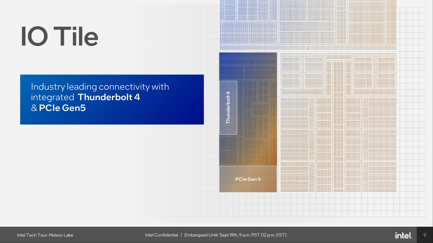
The I/O fabric, on the other hand, serves as the interconnection point for a range of on-chip devices that would traditionally reside in a discrete PCH. These encompass network controllers, security components, management engines, USB controllers, SATA controllers, and audio interfaces. Essentially, the I/O fabric functions as the PCI-Express root complex of the processor, with each I/O controller connected to it as they would be in a PCH setup. Additionally, an offshoot of the I/O fabric extends to the I/O tile, housing the processor’s PCI-Express PHY, USB4 controller, and Thunderbolt interface.
The I/O tile plays a pragmatic role, housing the processor’s physical layer interfaces like PCI-Express, Thunderbolt, and USB4. Essentially, it’s an extension of the SoC tile. Intel’s decision to have a separate I/O tile hinges on adaptability; it permits diverse I/O tile sizes to suit various processor models. The showcased I/O tile exemplifies the highest configuration, boasting abundant PCIe lanes, USB4, and Thunderbolt interfaces tailored for “Meteor Lake.” Lower-tier editions may adopt smaller I/O tiles with reduced PCIe lanes and without Thunderbolt. Likewise, Compute tiles may vary in dimensions, accommodating fewer P-cores for streamlined setups.
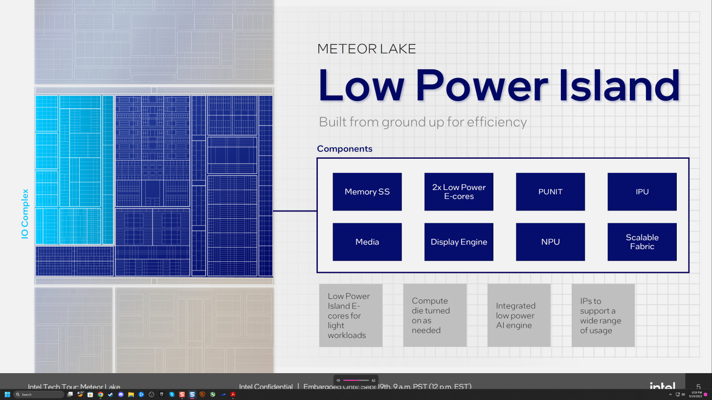
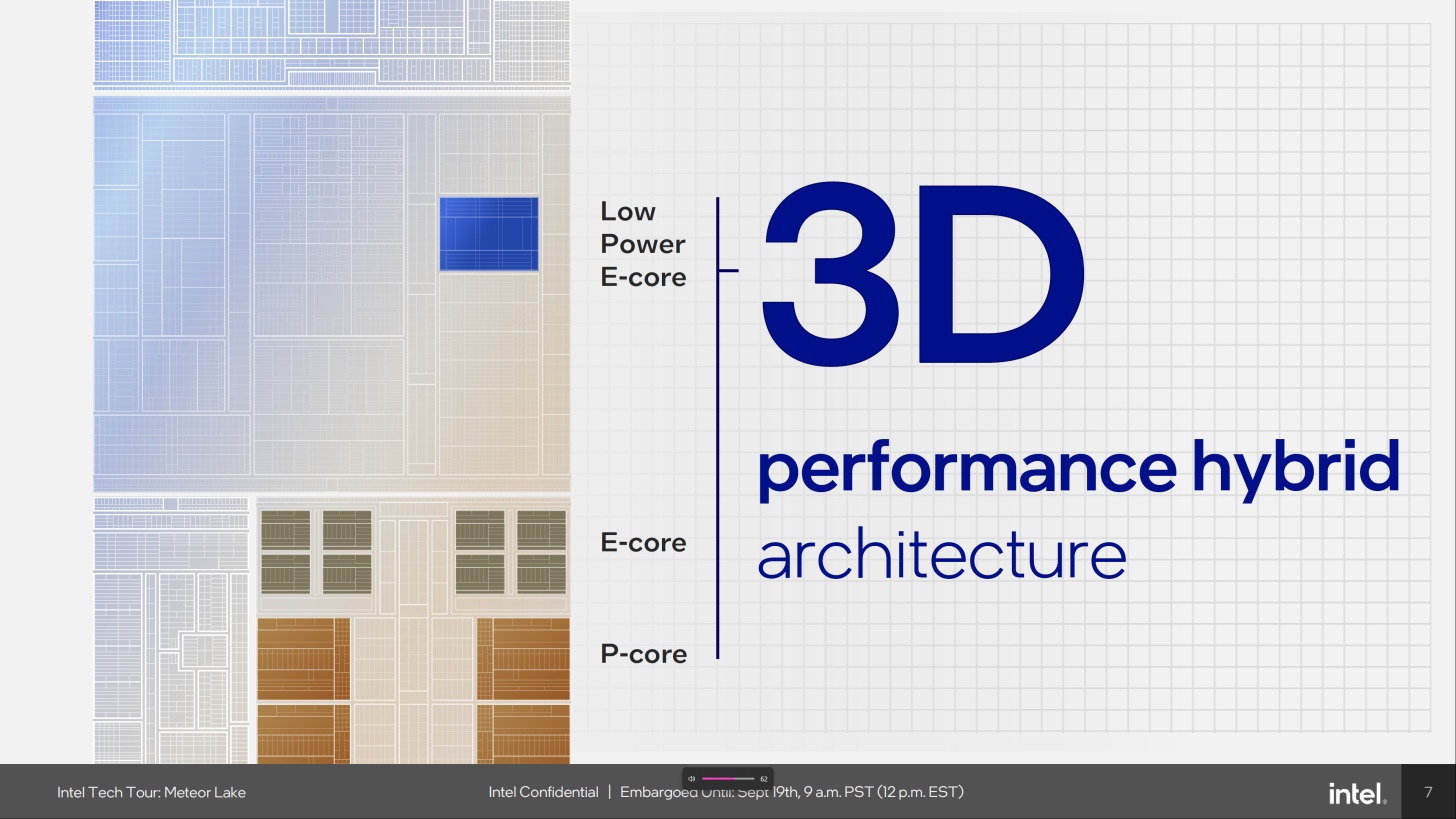
Intel’s Meteor Lake introduces a tiered CPU core hierarchy. The Compute tile houses the P-cores and E-core clusters, which share an L3 cache. Furthermore, another E-core cluster is positioned on the SoC tile, dubbed the Low Power Island E-cores. These E-cores, built on the Crestmont cores like their Compute tile counterparts, operate autonomously with an exclusive L2 cache serving the four cores.
The Low Power Island E-cores are fully integrated into the core count, appearing as logical processors in the OS and being monitorable through Windows Task Manager. They maintain the same ISA as the E-cores on the Compute tile. This arrangement serves two primary purposes: locating x86 cores in proximity to other on-die controllers, particularly the NPU, and enabling Intel to power down the Compute tile during periods of inactivity, resulting in substantial power conservation and something I’d have expected to have been a feature of Alder Lake and Raptor Lake which unfortunatelyt wasn’t the case. Thankfully Meteor Lake brings it to the table.
Intel NPU (Neural Processing Unit) and AI Boost
Much of Intel InnovatiON 2023 focused on AI and many of those that demo’d on-stage were highlighting the capabilities of their applications with powered by AI while leveraging Meteor Lake systems.
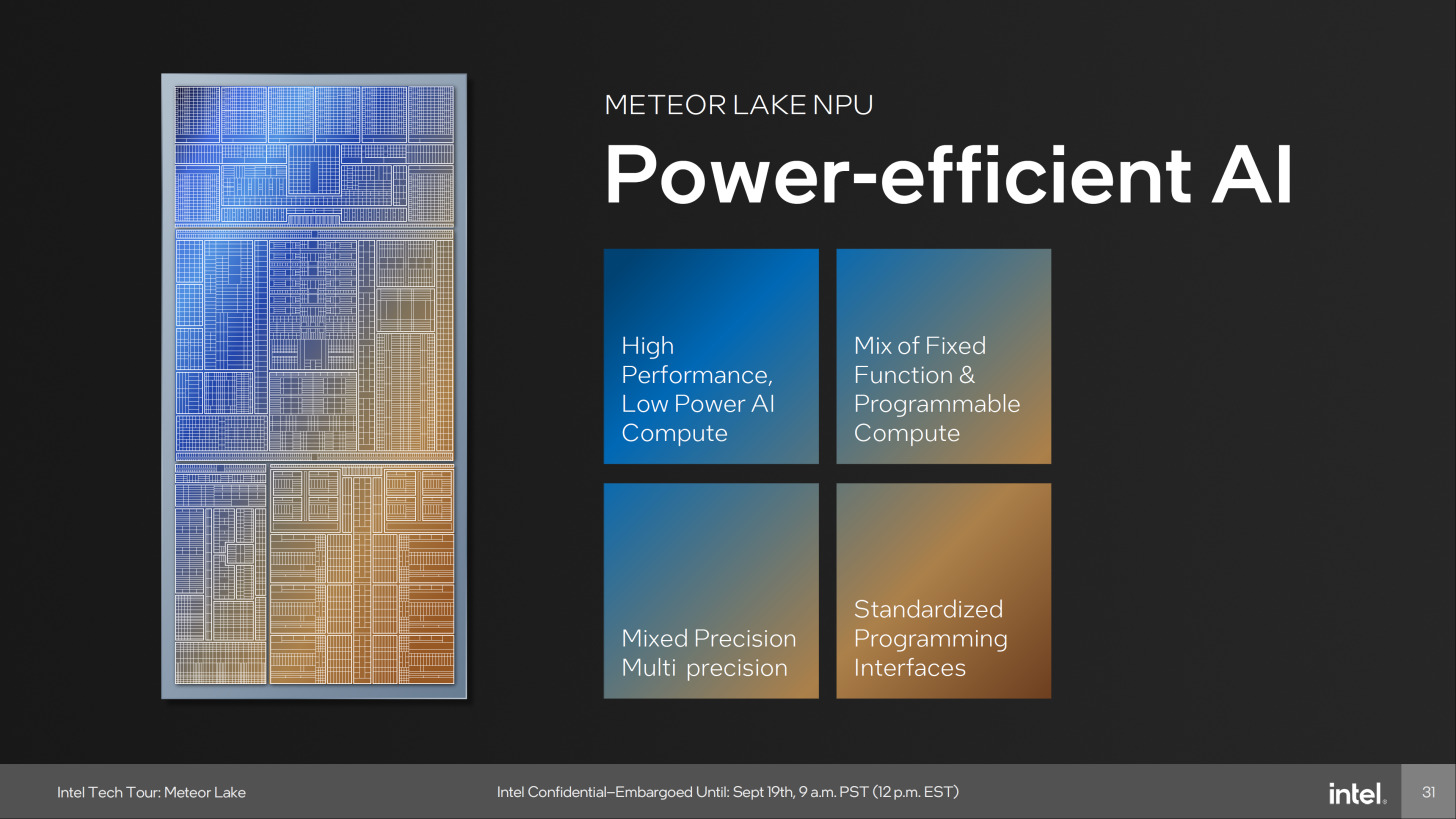
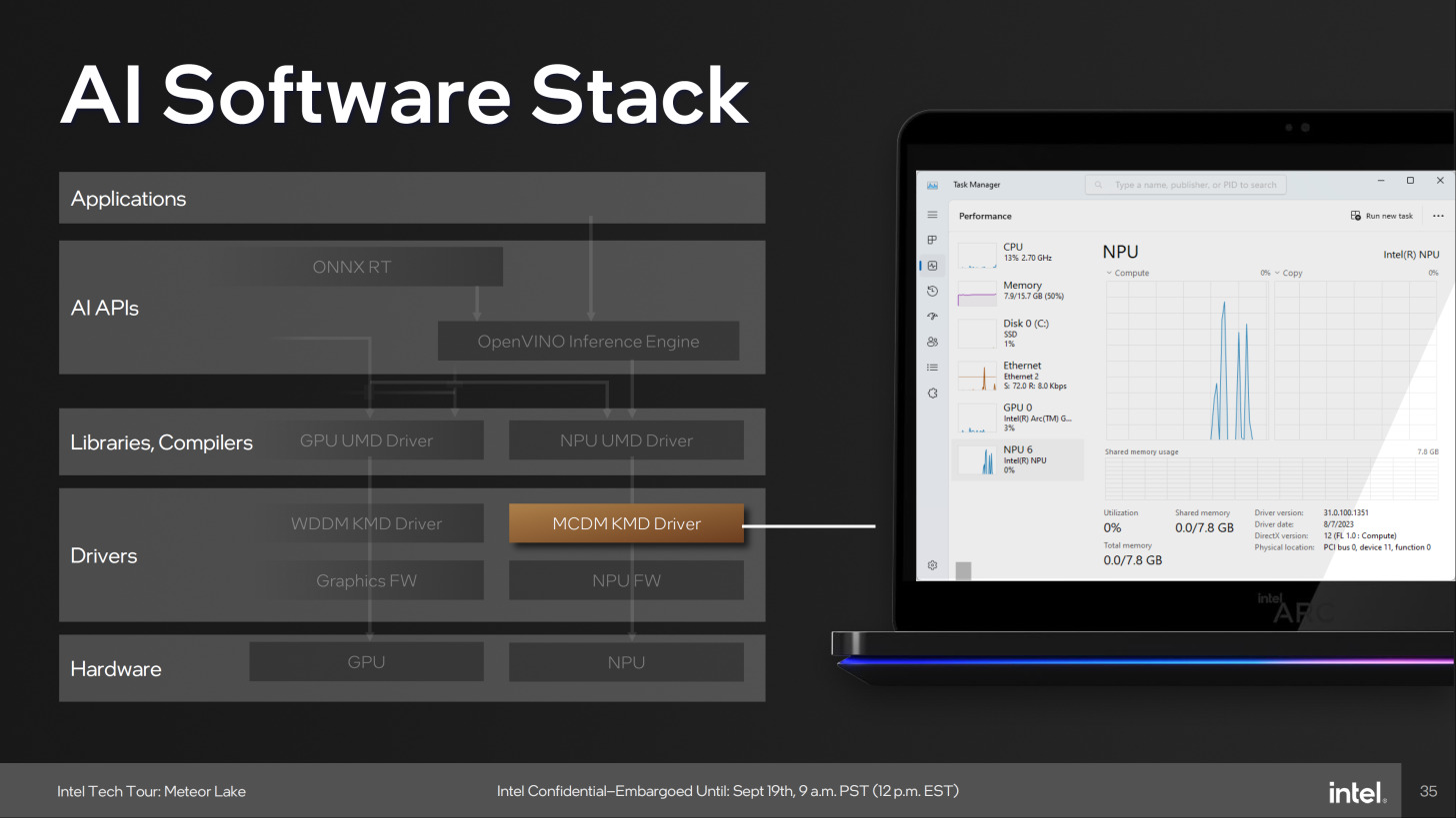
All processors based on Meteor Lake will feature an NPU (neural processing unit) located in the SoC tile. This NPU provides robust AI inference acceleration, following Microsoft’s MCDM driver model.
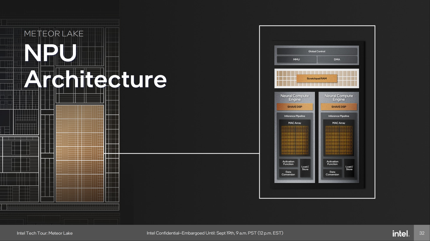
Within the NPU reside four primary hardware components: the Global Control, a memory mapping unit (MMU) with DMA capability, a compact scratchpad RAM, and two NCEs (neural compute engines). Each NCE encompasses a programmable DSP and an inference pipeline featuring the pivotal MAC array. This array consists of logic components that expedite matrix multiplication and convolution in both INT8 and FP16 formats, housing up to 2,048 MACs per cycle. Moreover, each NCE integrates two VLIW programmable DSPs capable of handling a wide range of data types, from INT4 to FP32.
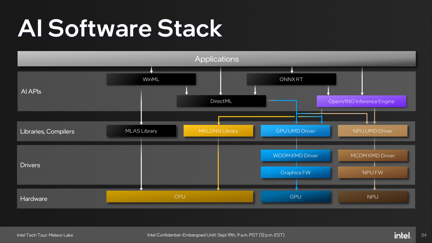
The NPU’s hardware capabilities are complemented by an extensive AI Software Stack, encompassing APIs such as WinML, DirectML, and ONNX RT, along with the OpenVINO inference engine. Various libraries and compilers are included in the stack, like MLAS and MKLDNN Library, which leverage AI acceleration features, and the Redwood Cove ISA (DLBoost) of the Compute Tile. The NPU’s power-efficient AI processing, hardware standardization, and uniform performance across all Core processor SKUs based on Meteor Lake justify its development.
Intel Xe Graphics on Meteor Lake
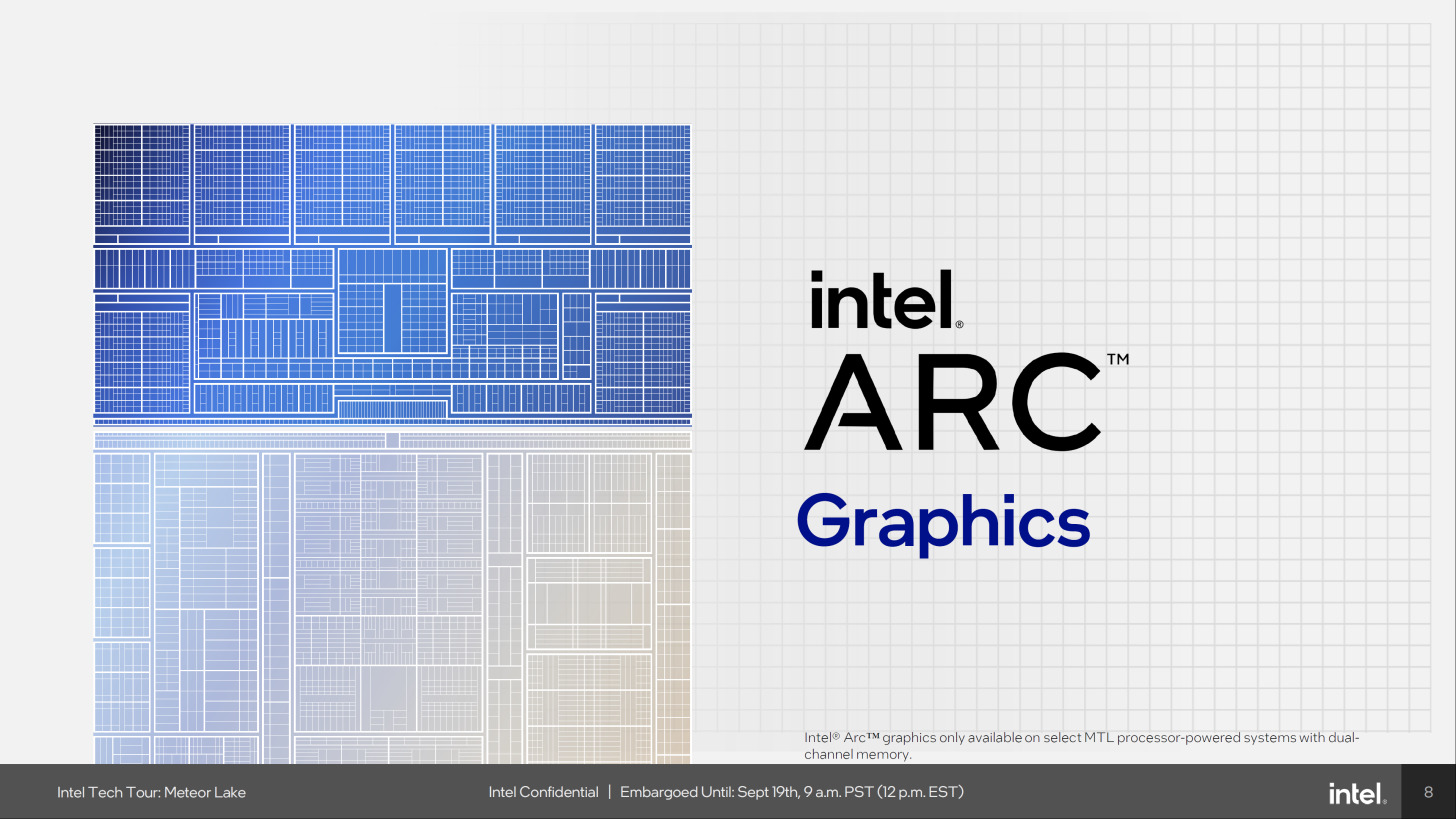
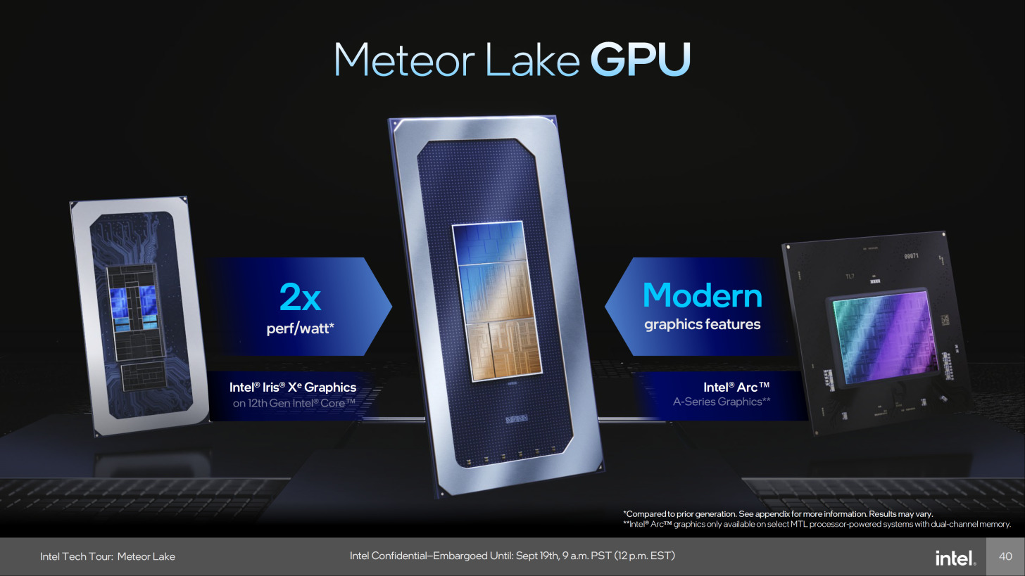
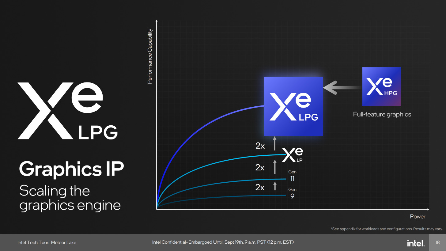
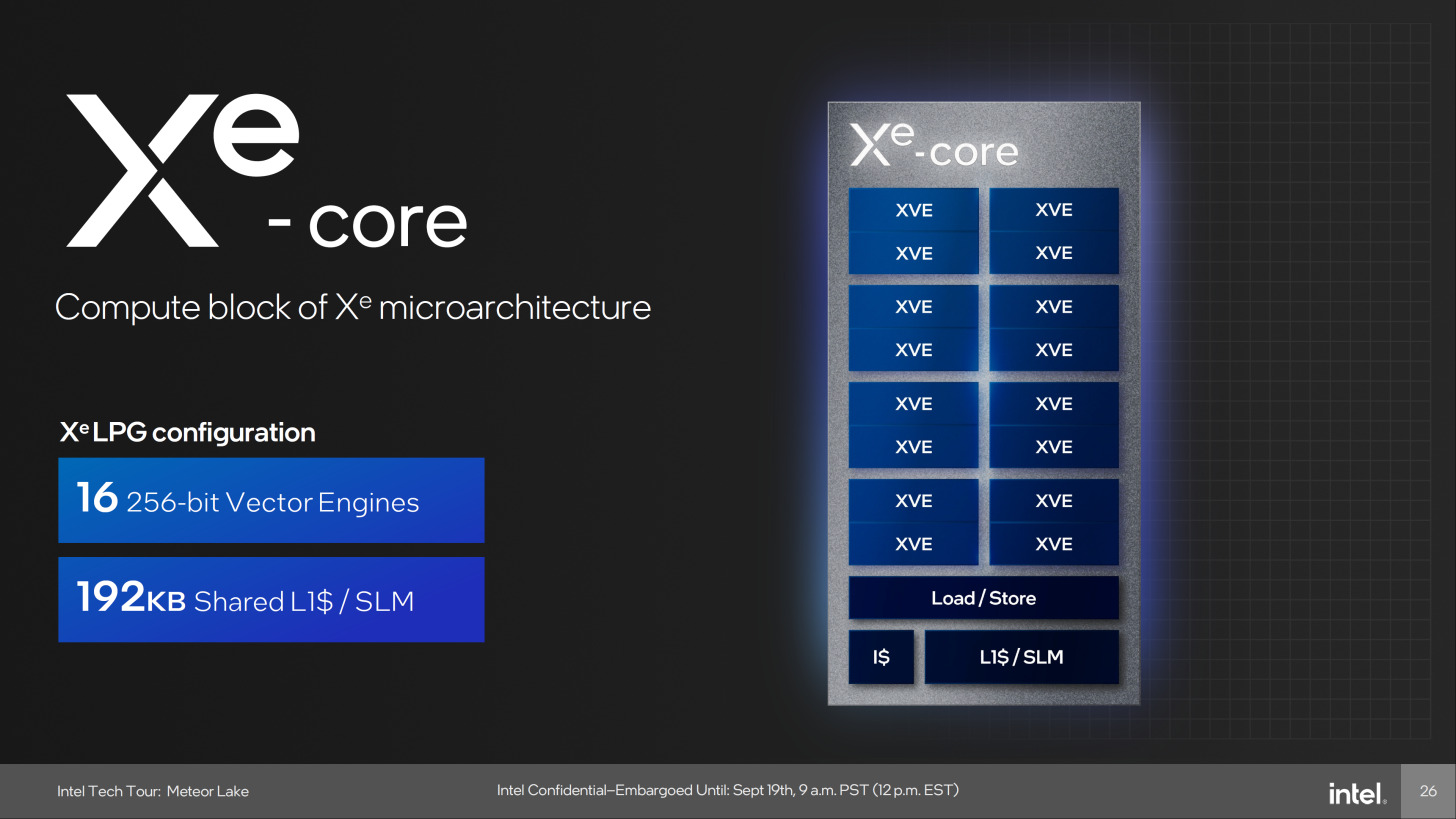
While its not Arc Graphics outright, Xe-LPG is a foundation of Xe-HPG is the bedrock of Arc Graphics. Anyway, focusing on Meteor Lake’s IGP and its graphics tile, this generation represents a notable shift in graphics processing. The iGPU is divided into three tiles: the Graphics tile, boasting advanced DirectX 12 Ultimate capabilities, including real-time ray tracing, while the SoC tile houses media accelerators and the display engine, all built on Intel 7. The I/O tile takes care of DisplayPort and HDMI interfaces.
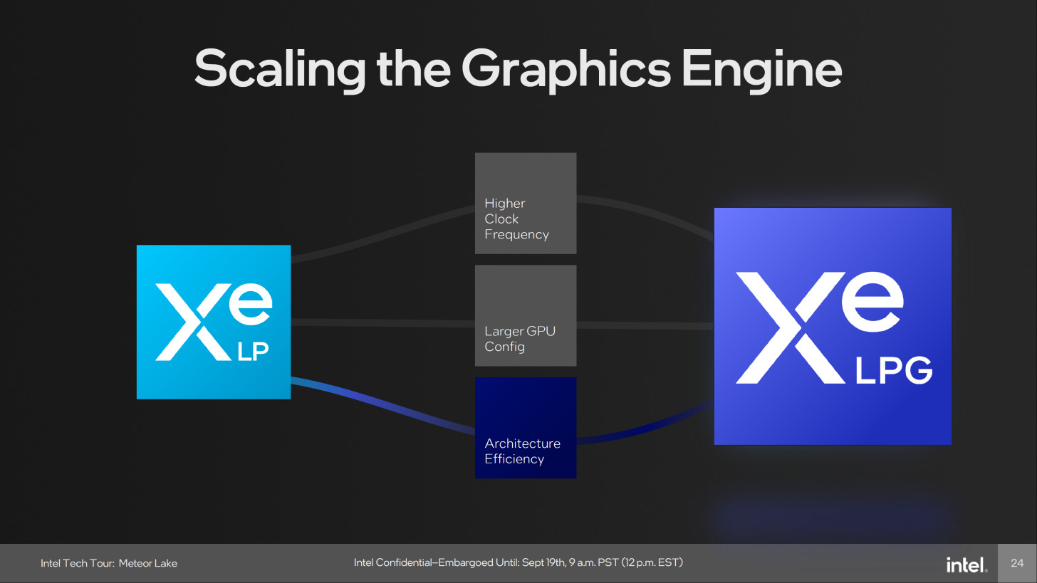
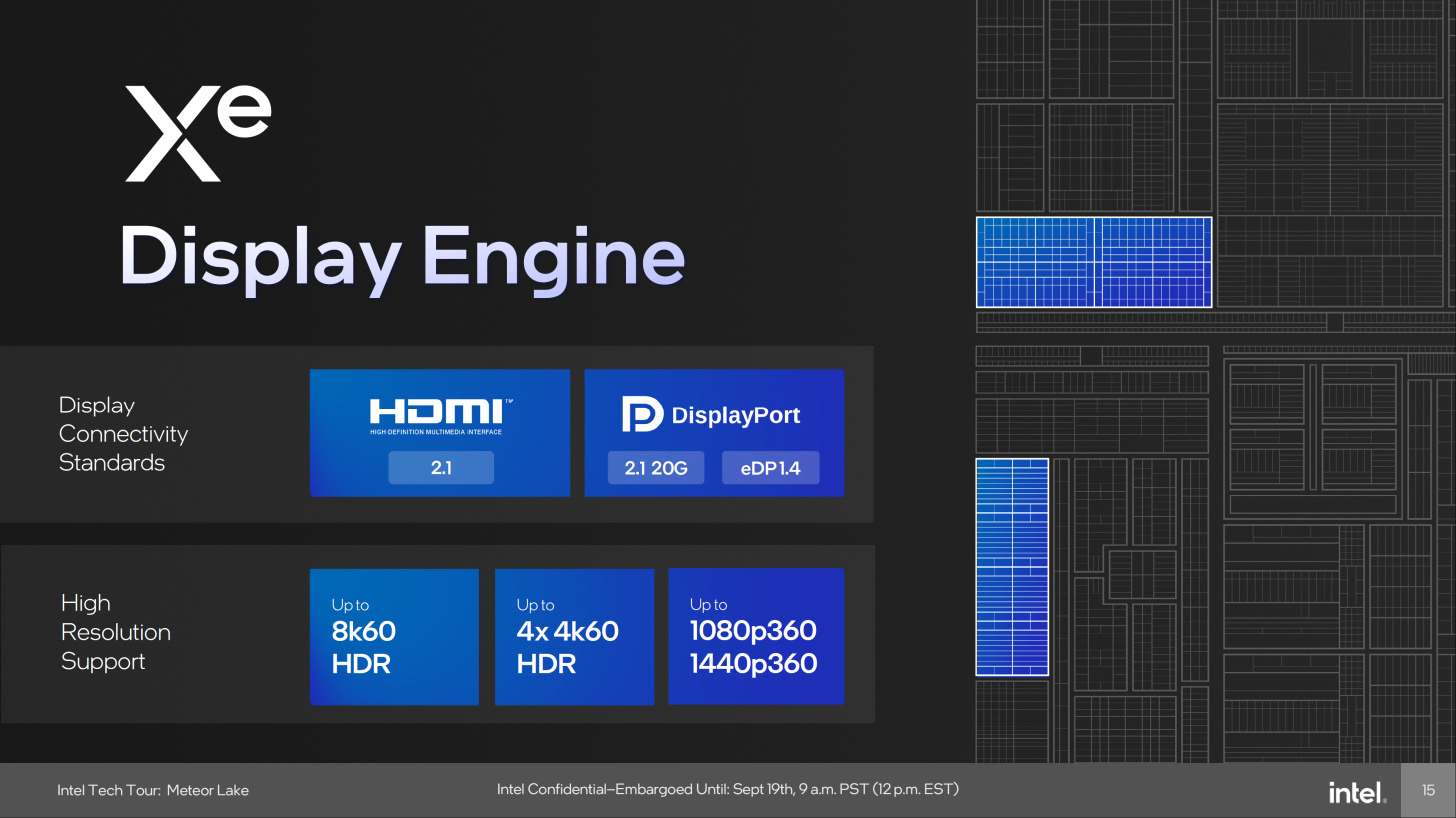
The Xe-LPG graphics architecture brings enhancements to Intel’s iGPUs. With a maximum configuration of 8 Xe cores, or 1,024 unified shaders, it offers higher clock speeds and architectural efficiency. The Xe Display Engine in the SoC tile supports impressive resolutions, and the Xe Media Engine handles video formats like VP9, AV1, HEVC, and AVC, supporting up to 8K resolution and HDR.
Moreover, the Xe Display Engine introduces power-efficient features like Burst Fill and Panel self-refresh. Intel’s Meteor Lake brings a substantial boost to integrated graphics, targeting more immersive and efficient visuals.
Intel 4 Process, Packaging and What to Expect
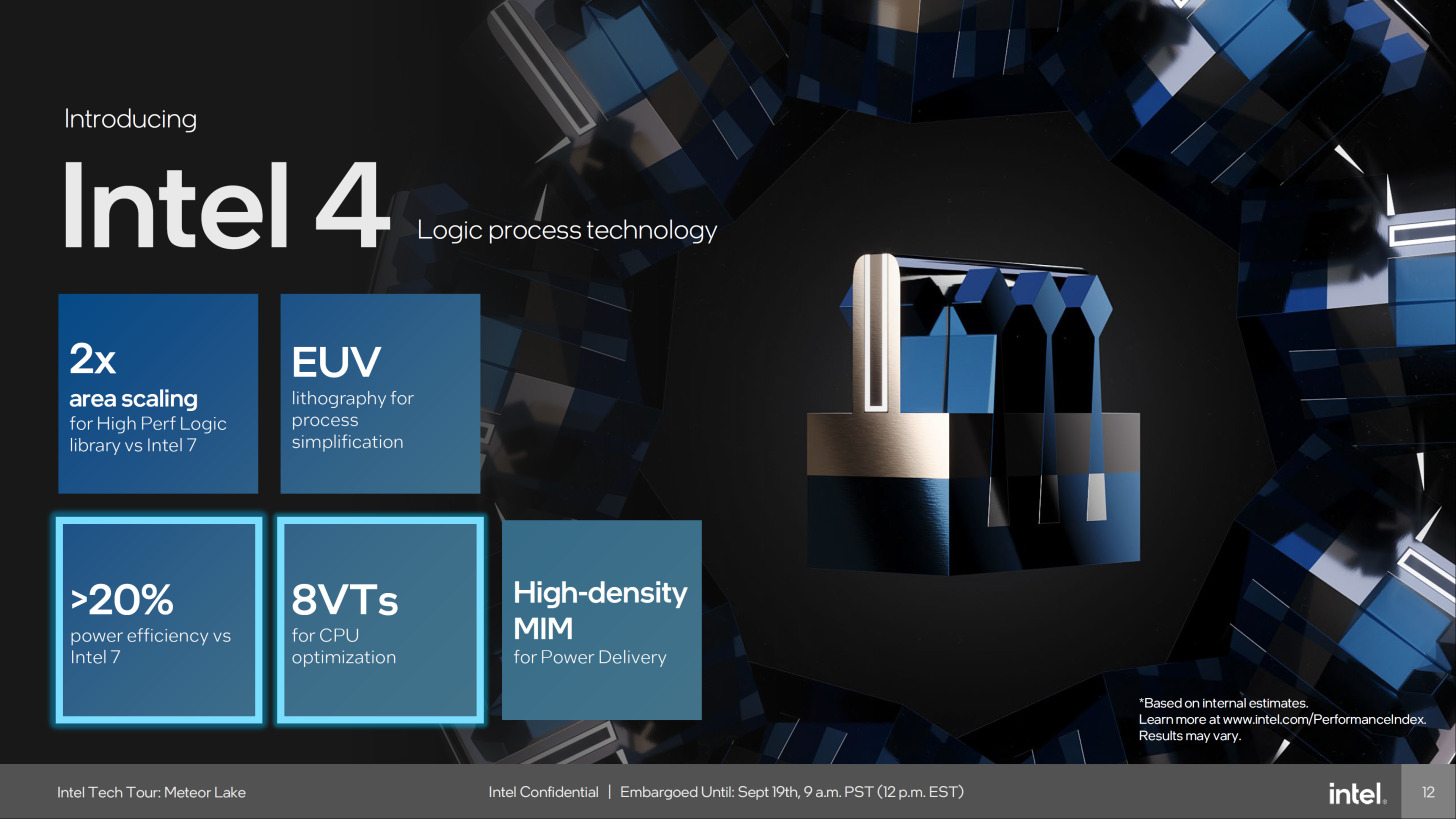
As we wind this overview down, we’ll close it with a brief overview of Intel 4, Intel’s process node for Meteor Lake and is intended to compete with TSMC’s N7. Intel 4 uses EUV lithography, ASML’s pride-and-joy and a technology that the world’s total install-base comprises of around 50% within TSMC’s facilities. EUV lithography allows Intel to catch-up to TSMC and gives significant improvements over Intel’s older process.
As already mentioned, Intel’s Meteor Lake is packaged using Foveros technology and while Intel’s demo video for Foveros makes it look like a Lego kit, stacking titles on the substrate requires far greater care and precision especially at scale and with the tiles sourced from various other foundries, a slew of rigorous testing is needed to achieve the best possible results from the package process.
Theory Time
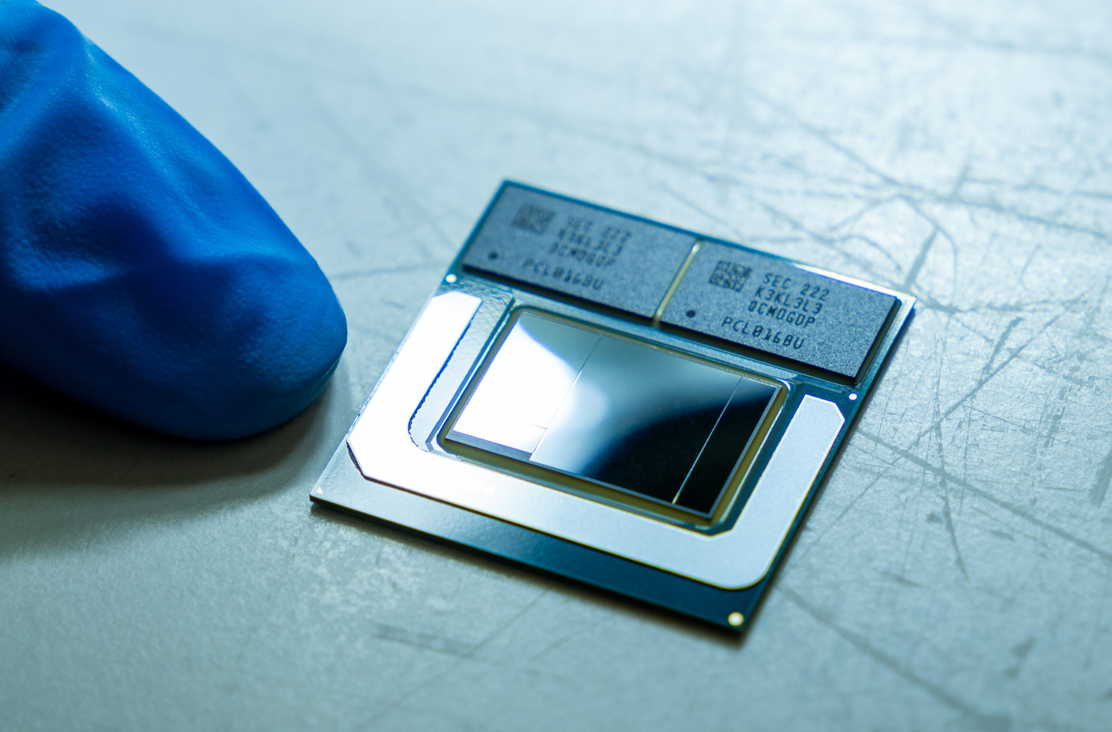 So what can we expect from Meteor Lake? Well, its going to arrive on systems on December 14, 2023 which would probably have its formal announcement with partners during CES 2024 where actual products would be ready for hands-on demos and probably reviews. The actual applications would widely vary as well as we don’t have actual SKUs announced yet.
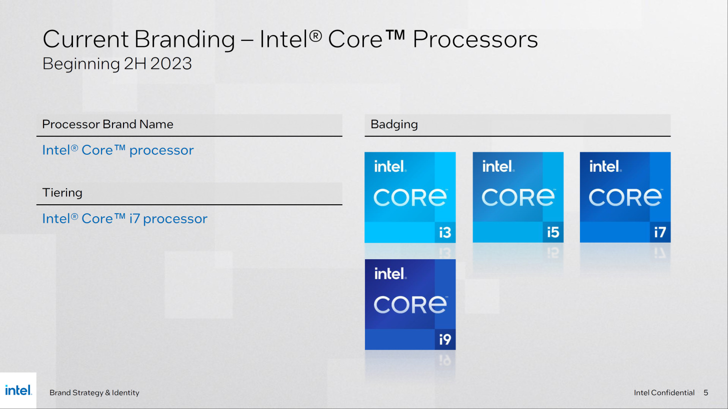
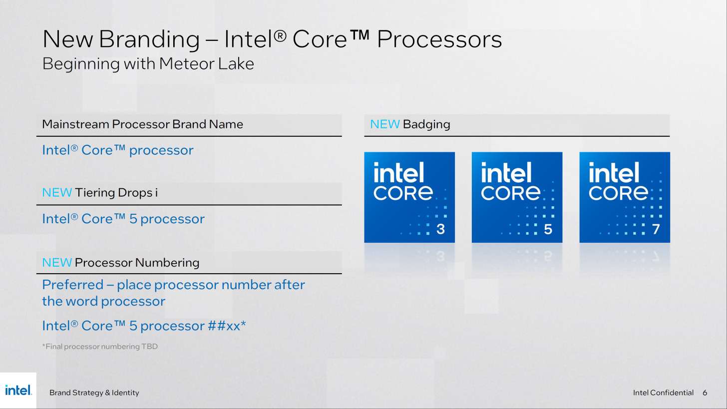
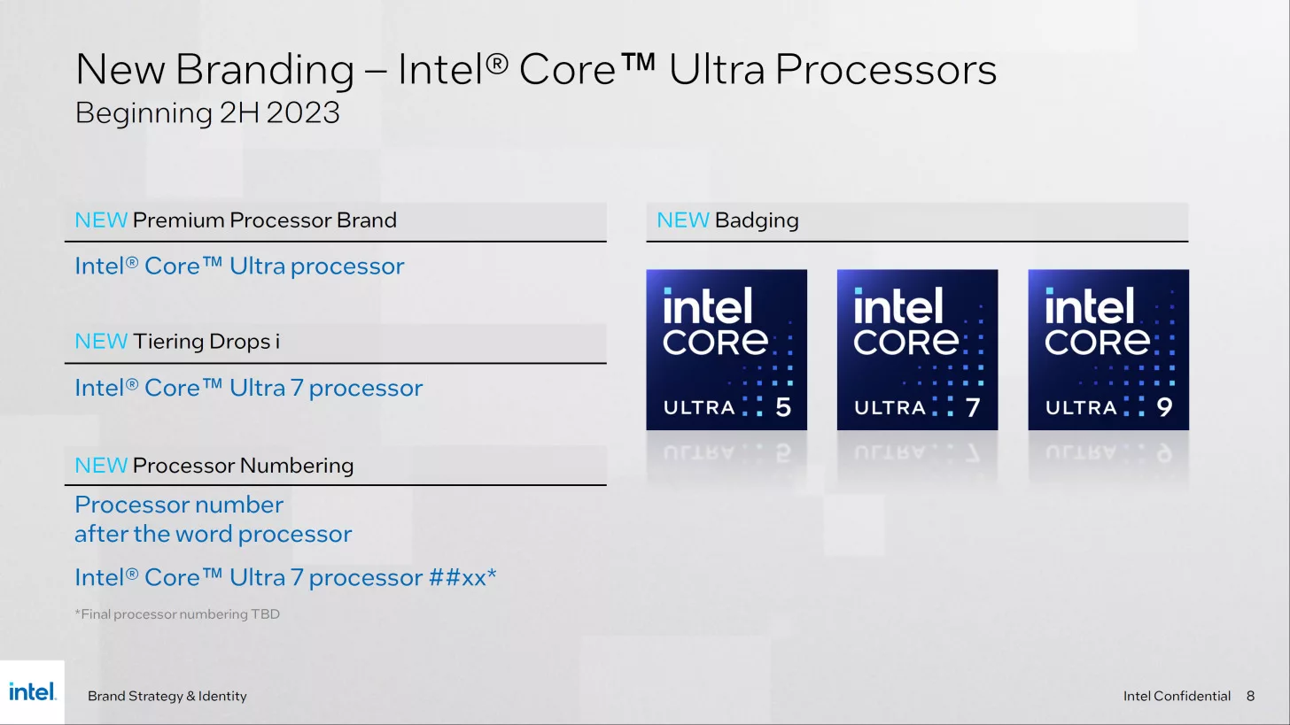
What is currently announced is the formal debut of Intel’s new Core branding which drops the “i” in favor of just a number. With Meteor Lake comes debut of the Intel Core 3, the Intel Core 5 and the Core 7 SKUs. Intel’s Core Ultra branding will also debut in H2 of 2023 but not during this announcement. This seems to be in-line with the announcement of the Raptor Lake Refresh for desktop, which is currently dubbed under codename “next-Gen Core” CPUs. Much like their current desktop counter parts, Intel Core Ultra parts would seem to fit the billing of the K-series SKUs but nothing right now is official.
Under the Intel Core Ultra series will have the Intel Core Ultra 5, Intel Core Ultra 7 and the Intel Core Ultra 9. While Intel can go with Core Ultra 9 14900K on the desktop and then Core 7 15900H on Meteor Lake, this will be very confusing and I would rather just wait for the official announcements than make some half-ass guesses.
Going back to Meteor Lake itself, its long been rumored that the new architecture will max out at 6 P-cores but have a significant amount of E-cores and with the Low Power Island able to power off other cores, its going to be really exciting to see how it translates to actual real-world power draw and battery drain.
The real challenge would be the transition to desktop with Intel already putting up 125W notation for power draw which only leaves us how Meteor Lake will translate that to desktop performance in both daily use, AI-accelerated appication and gaming.
We look forward to that day. As always, follow us on Facebook for more in-depth discussions on CPUs and more.


