In its Intel Accelerated event, the company revealed its roadmap for its process nodes until 2025. CEO Pat Gelsinger ushered in his first months in office by stating that Intel will regain its product leadership by 2025 and today we now see that plan in detail with Intel’s next five generations of process nodes being disclosed during the Intel Accelerated event.
IDM2.0 at Work
Most of us understand Intel IDM2.0 strategy as just a project naming but key to that strategy is a 3-step process that will help guide the company in developing process technologies to advance their active 10nm production while utilizing foundry services from other companies like TSMC to create their products to maintain their processor line which is a huge chunk of Intel’s profit maker. Lastly Intel’s new venture, Intel Foundry Service or IFS, where in Intel is providing their manufacturing capabilities for other businesses for semiconductor contract manufacturing.

This strategy allows Intel to perfect its internal process which it can later offer to its Intel Foundry Services (IFS) customers while letting contract manufacturers to manufacture their own products. Look at it as Intel cutting back on its own internal manufacturing to make room for R&D while they develop the process which will eventually get them back to their leadership goal by 2025. Leading this plan is Dr. Ann Kelleher, SVP and GM of the Technology Development.
Intel’s 2025 plan is targeting performance per watt with peak performance still a key part of developing that strategy.
Intel Node Naming Streamlined, Going Smaller than a Nanometer
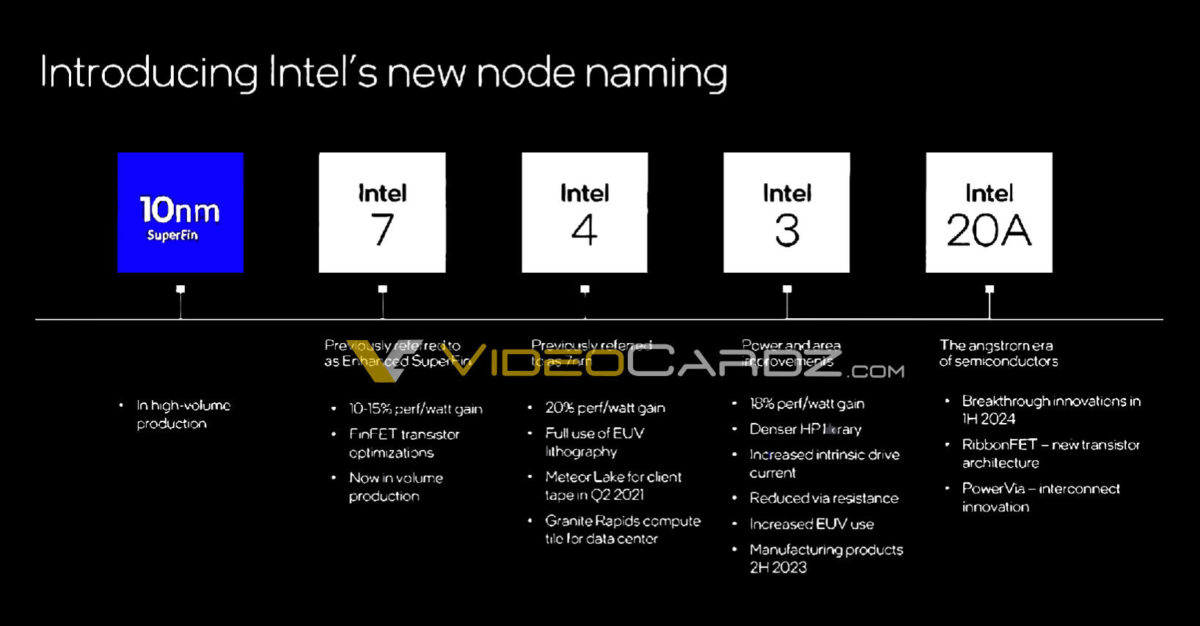
Intel has long been synonymous with their seemingly eternal node sizes. In an industry where TSMC has proliferated a fixed node name from its process scale, the progression is natural and easy to recall. Intel will be adopting a similar strategy in node naming and is disclosing their new naming going from their current conventions to a new, more discernible convention.
- 2020 – Intel 10nm SuperFin (10SF): this is the current-generation we have to this day with Intel Tiger Lake and Intel Xe-LP graphics. Intel will keep the naming for this generation.
- 2021 – Intel 7: Intel’s 10nm Enhanced Super Fin (10ESF) will now be referred to as Intel 7 and will be the node in which Alder Lake and Sapphire Rapids will be based on. This node targets a 10-15% performance improvement over the previoous 10SF node thanks to transistor optimization. This node is currently active in production with Alder Lake.
- 2022 – Intel 4: Intel’s 7nm node announced early 2021 and intended for a 2023 target for Meteor Lake. The silicon is already in testing and targets a 20% performance per watt improvement versus Intel 7. This node will use compute tiles.
- 2023 – Intel 3: A further development in EUV utilization, this node is aimed at further modularizing Intel’s strategy and is expected to ramp up for production by late 2023. Intel 3 is target an 18% performance per watt lead over Intel 4.
- 2024 – Intel 20A: The debut of the Angstrom unit, with 10A equivalent to 1nm. Formerly Intel 5nm, not much details is revealed for this node except this is when Intel will debut RibbonFET and PowerVia.
- 2025 – Intel 18A: Intel expects to receive ASML’s High-NA machines prior to work on this node. Intel is claimed to be the first partner to receive High-NA machines capable of the intricate lithography requirements of this scale. By this point, Intel is expecting unquestionable process leadership.
With relation to Intel Foundry Services, Intel 3 and Intel 20A will be available for customers but the other nodes are currently unknown if they’ll be made available for IFS customers as well.
By the release of Alder Lake later this year, we will have Intel 7 node products available with Xe-HP, Xe-HPC and Raptor Lake following soon after. After which no target products has yet been announced for Intel 4 onwards. Intel won’t disclose product release timeframes perhaps to avoid potential negative feedback when they publicly disclose timeframes and then meet delays.
Nanometers Isn’t What it Is Exactly in the Foundry Business
Intel’s competitor, TSMC and Samsung, has been using smaller numbers to name their nodes to match parity. TSMC and Samsung are happily willing to give a new node a full number despite only being a half-node. A half-node can be described as a variation of a current node, not fully qualified to describe the changes as a major node change. Samsung will give the new nodes a smaller number while in Intel’s convention, it will give it a +. Admirable for Intel but given the Skylake 14nm++++++++++++ meme, its going to be their undoing if they kept it up.
Going Forward
At the end of the day, the products will speak for themselves as all these naming convention will just be marketing fodder. Still, with regards to end products, we won’t know until we see them as for customers, it’s going to be the performance that matters.
For Intel though, customers is a two-prong word one of which refers their CPU business while the other is intended for their IFS customers. Intel has recently announced that Amazon AWS and Qualcomm are now onboard as IFS customers, Intel’s initial step is in motion its going to be a while until we see this plan coming into fruition.
The complete webcast for the Intel Accelerated event is below:
https://www.youtube.com/watch?v=b0MKuaoxBMk


